Semiconductor front-end quantity testing equipment: Key products continue to break through, and domestic substitution is accelerating
Report produced by: Guohai Securities
The following is an excerpt from the original report
------
1. Quantity detection equipment is the key guarantee for chip yield
Quantity detection equipment is the key guarantee for chip yield
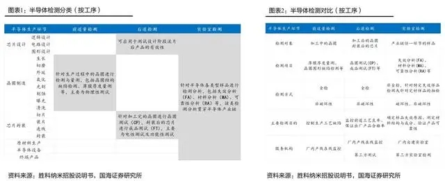
According to different processes, semiconductor testing can be divided into pre pass quantity testing, post pass quantity testing, and laboratory testing. Among them, pre pass quantity testing is mainly used in the wafer processing process, and currently, online monitoring of the production line in the factory is the main method; Post processing testing is mainly used for chip electrical and functional testing after wafer processing. Currently, it is mainly divided into third-party testing and on-site production line online monitoring; Laboratory testing mainly focuses on defect localization and fault analysis of failed samples. Currently, it is mainly divided into third-party laboratory testing and in-house self built laboratories.
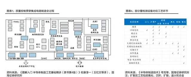
Quality control runs through the entire wafer manufacturing process and is a key guarantee for the yield of chip production.
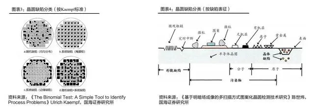
According to the Kaempf standard, wafer defects can be divided into random defects and systematic defects. Among them, random defects are mainly caused by particles attached to the wafer surface, and their distribution positions have a certain degree of randomness; System defects mainly come from systematic errors in photolithography masks and exposure processes, typically occurring in areas with sub resolution structural features, typically located at the same location in different chip regions on a single wafer.
According to defect characterization, wafer defects can be divided into morphological defects, pollutants, and crystal defects. Among them, morphological defects include small rough surfaces and pits, pollutant defects include pollutants such as organic and inorganic layers at the molecular level, ion and heavy metal defects at the atomic level, and crystal defects include silicon atom dislocation/dislocation, non silicon atom doping, etc.
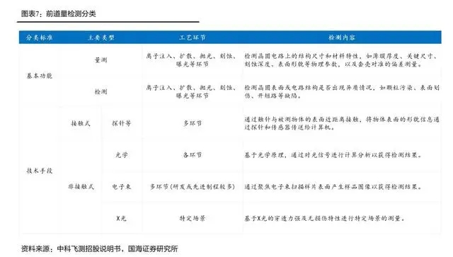
The front-end quantity detection equipment has two main functions: one is to ensure the mass production yield of the IC production line, and the other is to quantitatively monitor the production equipment, providing a basis for equipment acceptance and maintenance. The front-end quantity detection equipment can be classified according to basic functions, technical means, and defect types. This article will focus on comparing three types of equipment: optical/electron beam, bright/dark field, and patterned/non patterned.
Key comparison: Optical detection is currently the main solution
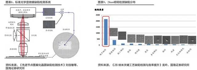
Optical detection has fast speed and no contact, and is currently the main detection technology. Optical detection technology obtains detection results through calculation and analysis of optical signals, which has advantages such as fast speed, non-contact, and easy online integration. According to the prospectus of Zhongke Feice, the detection speed of optical technology can be more than 1000 times faster than electron beam technology, and can be applied to all advanced processes at 28nm and below. It has been widely recognized by wafer fabs in terms of technological maturity, universality, reliability, and is currently the main detection technology for semiconductor quality control. According to the prospectus of Zhongke Feice, the global optical detection technology market size in 2020 was 5.75 billion US dollars, with a market share of 75.2% in quantity detection equipment. However, traditional optical detection techniques are limited by Rayleigh scattering in their detection principles, making it difficult to ensure high sensitivity to advanced node wafer defects. Moreover, their detection results often contain a large number of noise defects (non lethal defects), which can interfere with the detection of lethal defects.
Key comparison: Electron beam detection is suitable for high-precision scenarios
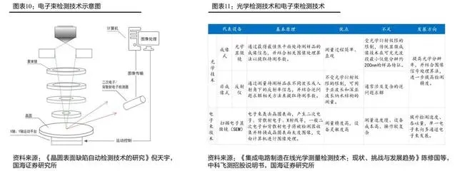
Electron beam technology has high detection accuracy, but the speed is slow and the equipment cost is high. Electron beam detection technology is the process of focusing an electron beam to a certain detection point, scanning the surface of a wafer point by point to generate images and obtain detection results. The wavelength of the electron beam is much shorter than that of light, and the resolution of the electron beam microscope is higher, with measurement accuracy superior to optical technology; However, the measurement speed is slow and the equipment cost is high. Considering that electron beam detection usually receives secondary electrons excited by incident electrons, it is impossible to distinguish depth information with three-dimensional features. Therefore, some detection methods cannot use electron beam technology and mainly use optical detection techniques, such as three-dimensional morphology measurement, photolithography and multi-layer film thickness measurement. According to the prospectus of Zhongke Feice, the global market size of electron beam detection technology in 2020 was 1.43 billion US dollars, with a market share of 18.7% in quantity detection equipment.
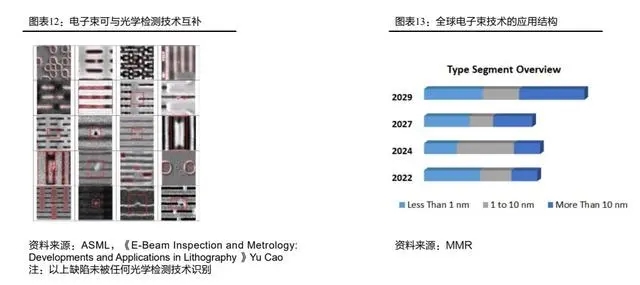
Electron beam and optical detection technology can complement each other. In practical applications, electron beam detection technology is partially applied in the research and development process, aiming to detect as many defects as possible, and partially applied in key area sampling and re examination, complementing optical detection technology. According to MMR, applications below 1nm will account for more than half of the global electron beam detection market in 2022. With the continuous development of advanced processes and complex devices, the advantages of electron beam detection technology are becoming increasingly apparent. The global electron beam detection market is expected to grow rapidly from 2022 to 2029, with a CAGR of 19.9%. The market size is expected to increase to 2.58 billion US dollars by 2029, and applications above 10nm will become the main market for electron beam technology.
Key comparison: Multi system combination may become a development trend
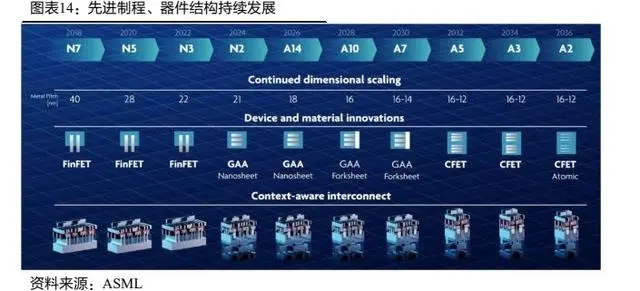
With the continuous development of advanced manufacturing processes, the complexity of IC materials and structures continues to increase. The defects to be tested have shifted from surface to three-dimensional distribution, the geometric structure has become increasingly complex, and the size is gradually approaching atomic level. Single defect detection technology is becoming increasingly difficult to adapt to, and the combination of multiple systems may become a trend in the development of detection technology.
Route 1- Traditional Optics: Optical detection technology based on bright and dark field illumination has been widely recognized by wafer fabs in terms of technological maturity, universality, reliability, and other dimensions. However, the detection principle is limited by Rayleigh scattering, making it difficult to ensure high sensitivity at advanced nodes. Therefore, signal-to-noise ratio analysis of different defects is particularly important.
Route 2- Multi electron beam: Multi electron beam imaging has high lateral resolution, but there is still a difference in detection rate compared to optical technology. The research hotspot is to strike a balance between system complexity, overall cost, and detection efficiency.
Route 3- Extremely short wavelength: For example, stacked diffraction imaging technology based on extreme ultraviolet and hard X-ray bands is expected to achieve 3D imaging of wafer surface and subsurface defects. However, the lack of desktop extreme wavelength light sources with high brightness, high coherence, and high stability is currently a key limiting factor.
Route 4- Structured Light Field: Fully explore the multidimensional intrinsic characteristics of light as a three-dimensional electromagnetic field (in addition to amplitude, frequency, phase, polarization state, orbital angular momentum, etc.), in order to maximize the sensitivity of defect detection.
Key comparison: High precision in bright field systems and fast speed in dark field systems
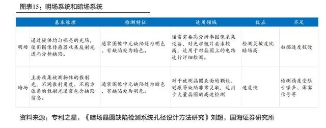
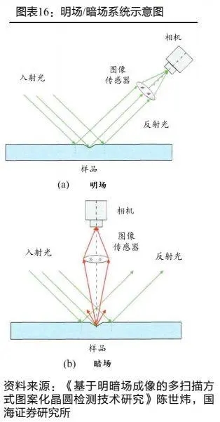
The dark field system mainly collects scattered light from the tested object and is suitable for high-speed detection of a large number of wafers. However, the scattered signal intensity is much lower than that of incident and reflected light, and noise has a significant impact on detection accuracy, directly determining the detection limit of the system; 2) The surface of the wafer is not completely smooth, and micro undulations can also generate scattered light (haze signal), which affects the detection accuracy.
The bright field system provides a uniform and bright light field, uses image sensors to collect reflected light and analyze defects. Compared with the dark field system, it has higher detection sensitivity and slower scanning speed, making it suitable for detailed inspection of wafer circuits.
The existing technology usually only matches one system, either bright or dark, because there is a significant difference in brightness between defect free and defective areas. Defect analysis is achieved by threshold judgment of the grayscale value of the graphics. Currently, dark field systems occupy the main market of wafer detection equipment.
Key comparison: Image detection mainly uses optical technology
Dark field optics is an important means of pattern free detection. Non graphic defect detection equipment is used to detect surface unetched wafers. The types of defects mainly include particle contamination, pits, watermarks, scratches, shallow pits, epitaxial stacking, CMP protrusions, etc. It is mainly used for: 1) defect detection in wafer manufacturing, process research and development, and final inspection process before wafer leaving the factory; 2) In the field of chip manufacturing, quality inspection of incoming materials, process control (thin film, CMP, etc.), detection of contamination on the back of wafers, monitoring of equipment cleanliness, etc; 3) In the field of semiconductor equipment manufacturing, defect detection in process research and development, and process quality evaluation of equipment. For bare crystal wafers, particles and scratches on the wafer are the main forms of defects and have high sensitivity in high-frequency scattering components. Therefore, optical detection methods such as dark field microscopy are important detection methods.
Image detection mainly uses bright field optical technology. There are graphic defect detection devices used to detect etched patterns on ICs. The types of defects include not only surface defects such as nanoparticles, dents, protrusions, scratches, wire breaks, bridges, but also sub surface and internal defects such as voids and uneven material composition. Bright field optical detection technology is mainly used. Due to the complexity of patterns and the diversity of materials, the detection of graphic defects becomes more complex and challenging. The importance of high-precision instruments, advanced modeling methods, and image post-processing algorithms continues to be highlighted.

The localization rate of core components needs to be improved
The localization rate of components such as light sources, lenses, and cameras needs to be improved. According to the prospectus of Zhongke Feice, the company's required raw materials mainly include motion and control systems, optics, electrical, machined parts, mechanical standard parts, and other components. Core components include light sources, lenses, cameras, detectors, optical components, sample stages, EFEM, robotic arms, etc. Among them, motion and control system components such as robotic arms are mainly purchased from overseas suppliers such as Japan, while optical components such as detectors are mainly purchased from overseas suppliers such as Germany.
2. The domestic market for quantity testing equipment is expected to develop rapidly
Driver 1: The global semiconductor market is gradually recovering
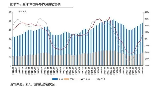
The global semiconductor market is expected to accelerate its recovery and growth in 2024. According to SIA data, the global semiconductor industry's sales in November 2023 were $48 billion, a year-on-year increase of 5.3%. After experiencing six consecutive months of narrowing year-on-year decline, it achieved year-on-year growth for the first time this year, with nine consecutive months of month on month growth. According to the semiconductor industry vertical and horizontal official account, IDC raised the forecast value of the global semiconductor market size in 2023 from $518.8 billion to $526.5 billion, and the 2024E market size from $625.9 billion to $632.8 billion, with a year-on-year growth of 20.2%. The global semiconductor market is gradually warming up, and is expected to accelerate its recovery from 2024. The short-term recovery is mainly driven by the gradual warming of consumer electronics, benefiting from the machine change boom after the release of Huawei, Apple and other new products. The long-term development is driven by emerging growth points such as automotive, data centers, industry and AI.
Driving force 2: continuous expansion of wafer fabs in Chinese Mainland
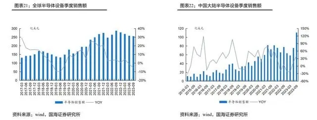
Chinese Mainland strengthened investment in mature process capacity. Taking SMIC International as an example, the third quarterly report of SMIC International raised its annual capital expenditure to about US $7.5 billion in 2023, an increase of about 18% year on year. In 2022, the global share of 12 inch wafer capacity in Chinese Mainland will be 22%, and it is expected to increase to 25% in 2026. The domestic semiconductor equipment market is expected to grow steadily in the long run due to the demand recovery of the semiconductor industry and the continuous expansion of wafer factories in Chinese Mainland. According to SEAJ data, the sales volume of semiconductor equipment in Chinese Mainland in 2023Q1-Q3 is 24.47 billion US dollars, up 11.7% year on year, and 42.2% year on year in 2023Q3.
Driving Force 3: Advanced Process Boosts Equipment Investment Demand
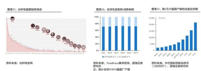
The value of advanced process corresponding quantity detection equipment is expected to double. AI chips have high requirements for performance, power consumption, and cost, and have significant advantages in advanced manufacturing processes. At the same time, with the development of automotive intelligence, traditional chips such as MCUs are no longer able to meet market demand. The gradual enrichment of automotive chip functions is expected to help accelerate the development of advanced manufacturing processes. With the advancement of chip manufacturing processes, equipment investment costs will show a significant upward trend. According to SMIC's prospectus (July 2020), taking the 5nm process as an example, its investment cost can reach tens of billions of dollars, more than twice that of 14nm and about four times that of 28nm. Advanced manufacturing processes will require higher levels of process control, and the value of testing and measuring equipment is expected to double.


Please first Loginlater ~