How to test the transition from circular to non circular wafer shape - Enterprise website
Wafers are an important component of technology, and without them, advanced technology will stagnate. So, how to determine the quality of the finished wafer after it is manufactured?
How to test the transformation of wafer shape from circular to non circular
Wafers are an important component of technology, and without them, advanced technology will stagnate. So, how to determine the quality of the finished wafer after it is manufactured? In this article, the editor will introduce the testing methods of wafers and explore the shape changes of wafers. If you are interested in wafers, or if you are interested in the content to be introduced in this article, why not continue reading.
1、 Wafer material
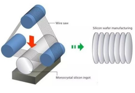
Silicon is refined from quartz sand, and wafers are made by purifying the silicon element (99.999%). Then, these pure silicon are made into silicon crystal rods, which are used as materials for manufacturing quartz semiconductors in integrated circuits. Through processes such as photo plate making, grinding, polishing, and slicing, polycrystalline silicon is melted and pulled out of single crystal silicon crystal rods, which are then cut into thin wafers.
2、 Wafer testing methods
Wafer testing is the process of needle testing each grain on a chip. A probe made of gold wire, as thin as hair, is installed on the testing head to make contact with the contact points on the grain and test its electrical characteristics. Unqualified grains are marked, and when the chip is cut into independent grains based on the grain unit, the marked unqualified grains are eliminated and no further process is carried out to avoid increasing manufacturing costs. After the completion of wafer manufacturing, wafer testing is a very important step. This test is the transcript of the wafer production process. During the testing process, the electrical capability and circuit functionality of each chip are detected. Wafer testing, also known as chip testing or wafer electrical testing. During testing, the wafer is fixed on a vacuum suction chuck and aligned with a thin probe electrometer, while the probe contacts each solder pad of the chip (as shown in the figure). The electric tester tests the circuit under the drive of the power supply and records the results. The number, order, and type of tests are controlled by computer programs. The testing machine is automated, so there is no need for operator assistance in the testing work after the probe electrical tester is aligned with the first wafer (manually or using an automatic vision system). The testing is aimed at the following three objectives. Firstly, identify qualified chips before the wafers are sent to the packaging factory. Secondly, evaluate the electrical parameters of the device/circuit for their characteristics. Engineers need to monitor the distribution of parameters to maintain the quality level of the process. Thirdly, the accounting of qualified and defective chips will provide comprehensive performance feedback to wafer production personnel. The positions of qualified chips and defective products on the wafer are recorded in the form of a wafer diagram on the computer. The old technology of the past applied a dot of ink on defective chips. Wafer testing is one of the main methods for calculating chip yield. As the area and density of chips increase, the cost of wafer testing increases. In this way, chips require longer testing time and more precise and complex power supplies, mechanical devices, and computer systems to perform testing work and monitor test results. The visual inspection system also becomes more precise and expensive as the chip size expands. The chip designers are required to introduce testing modes into the storage array. Test designers are exploring ways to simplify and effectively test the process, such as using simplified testing programs after chip parameter evaluation is qualified, and also testing chips on the wafer in an interlaced manner, or testing multiple chips simultaneously.


Please first Loginlater ~